Microelectronics Laboratory
Microelectronics Laboratories support one of the major areas of specialization in the Department of Electrical and Computer Engineering and Technology (ECET). In this facility students start with bare silicon wafer and use their design to fabricated their Integrated Circuit (IC) chip and electrically test their design. The laboratories are uniquely suited for teaching IC Fabrication, faculty member’s research, and research projects sponsored by industry and other funding agencies.
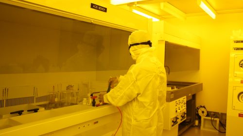
The central facility of Microelectronics Laboratory is a class 100 clean room areas, which occupies over 3,300 square feet. The clean room area is laid out into four zones, which are dry processing laboratory, photolithography laboratory, wet processing laboratory, and analytical laboratory. Service bays surround all the four sections of the laboratory just like semiconductor industry has for IC Fabrication, or it is a scaled down version of semiconductor industry fabrication facility. The entire clean room area is equipped with temperature and humidity controller. Ultrahigh purity gases are distributed throughout the laboratory using electro-polished stainless steel delivery system. The laboratory is equipped with centralized smoke, fire, and toxic air monitoring system to safeguard personnel against potential dangers. In addition, the laboratory is outfitted with automated gas cabinets with gas leak alarm system and deionized (DI) water delivery system. The laboratory has the equipment to support research and teaching in microelectronics materials growth, processing, device designing and material, and device characterization, and testing of IC chip. See Figure-1 for the floor plan of the Microelectronics Fabrication Laboratory.
The wet processing laboratory equipment include wet chemical hoods for acid and solvent, which are equipped with ultrasonic baths, quick dump rinser, deionized water baths with DI water resistivity monitoring probes, photoresist spinner, angle lapping machine, and spin drying units.
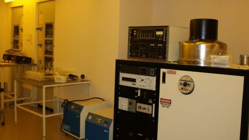
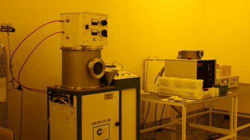
The dry processing laboratory equipment includes reactive ion plasma etching (RIE) system, plasma-enhanced-chemical vapor deposition (PECVD) reactor, e-beam and magnetron sputter deposited metallization systems, plasma ashing unit, and six tube furnaces configured for wet and dry oxidation, diffusion, and sintering.
In the photolithography laboratory, the optical tools are contact mask aligners and 0.7 Micron projection stepper system. The other major equipment are Quintel Contact Mask Aligner, and Quintel UV and IR contact Mask Aligner.
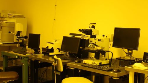
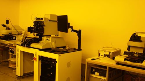
The analytical laboratory houses most recent tools for thin film measurement and characterization of devices fabricated on microchip. The major equipment in this area of the laboratory includes Ellipsometer, Nanoline measurement system, Nanospec, four-point probe, Keithley IV and simultaneous CV measurement system equipped with software for parameter extraction and plotting capability, HP parameter analyzer attached to probe station housed in an isolation chamber, high resolution microscope equipped with CCD camera and inspection microscopes mounted on oscillation free tables.
Deionozed (DI) water is supplied to the all areas of the laboratory through a DI-water system attached to the clean room. All gases used in IC chip processing, their delivery system is located in this area of the laboratory.
Some of the equipment was acquired through donation from UNISYS, IBM, 3M, and Honeywell, and funds from National Science Foundation (NSF) under Instrumentation and Laboratory Improvement (ILI) program, and funds from College of Science, Engineering and Technology (CSET).
Microelectronics Lab and other labs received $200K in FY 2018 from MinnState leverage fund and acquired power computer workstations for modeling and simulation research.
For more info or questions, please contact Dr. Muhammad Khaliq or Dr. Puteri Megat Hamari.
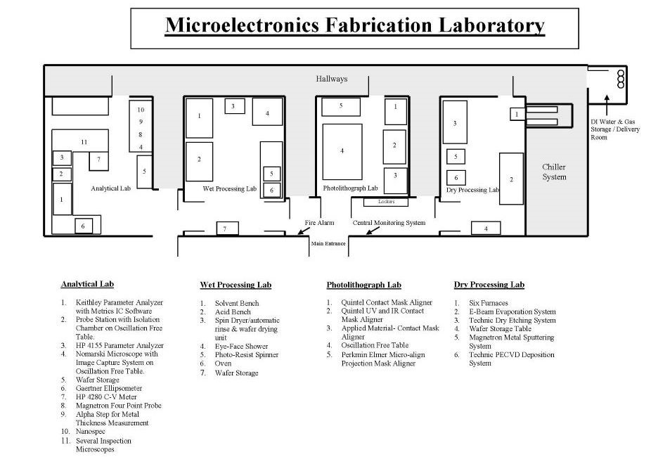
| Analytical Lab | Wet Processing Lab | Photolithograph Lab | Dry Processing Lab |
|---|---|---|---|
| 1. Keithley Parameter Analyzer with Metric IC Software 2. Probe Station with Isolation Chamber on Oscillation Free Table 3. HP 4155 Parameter Analyzer 4. Normarski Microscope with Image Capture System on Oscillation Free Table 5. Wafer Storage 6. Gaertner Ellipsometer 7. HP 4280 C-V Meter 8. Magnetron Four Point Probe 9. Alpha Step for Metal Thickness Measurement 10. Nanospec 11. Several Inspection Microscopes |
1. Solvent Bench 2. Acid Bench 3. Spin Dryer/ automatic rinse & wafer drying unit 4. Eye-Face Shower 5. Photo-Resist Spinner 6. Oven 7. Wafer Storage |
1. Quintel Contact Mask Aligner 2. Quintel UV and IR Contact Mask Aligner 3. Applied Material-Contact Mask Aligner 4. Oscillation Free Table 5. Perkmin Elmer Micro-align Projection Mask Aligner |
1. Six Furnaces 2. E-Beam Evaporation System 3. Technic Dry Etching System 4. Wafer Storage Table 5. Magnetron Metal Sputtering System 6. Technic PECVD Deposition System |